The demand for more efficient, compact, and specialized electronic components is ever-growing. Application-Specific Integrated Circuits (ASICs) have become critical to meeting these demands. Unlike general-purpose integrated circuits, ASICs are tailored for specific applications, offering superior performance and efficiency for targeted tasks.
Understanding ASICs: What Are They?
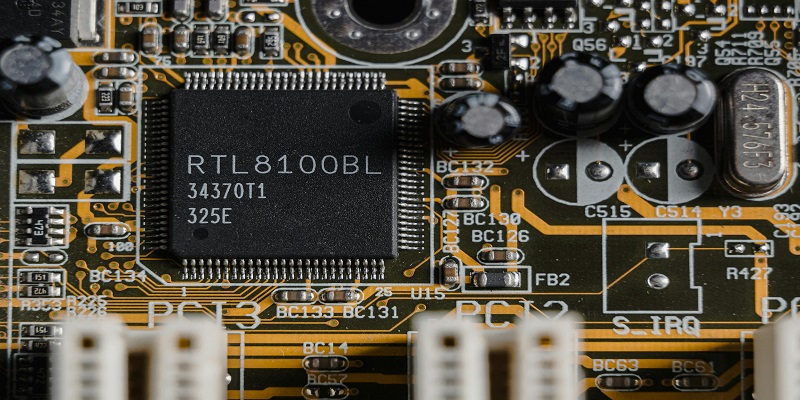
An Application-Specific Integrated Circuit (ASIC) is a type of semiconductor that is custom-designed for a particular application or function. Unlike general-purpose integrated circuits (ICs) such as microprocessors, which are designed to handle a wide range of tasks, ASICs are optimized for a specific application. This allows them to perform their designated function with greater efficiency, speed, and lower power consumption.
For example, ASICs are often used in consumer electronics, such as smartphones and gaming consoles, where they help to enhance performance and reduce power consumption. They are also widely used in industrial applications, including automotive systems, telecommunications, and medical devices. Essentially, ASICs are integral to any industry that requires specialized electronic components tailored for specific tasks.
The ASIC Design Process: A Step-by-Step Guide
The design of an ASIC involves several complex stages, each requiring meticulous attention to detail. Here’s a step-by-step overview of the ASIC design process:
Specification and Requirements Gathering
The first step in the ASIC design process is to define the specifications and requirements of the circuit. This involves understanding the specific application for which the ASIC is being designed and identifying the performance, power, and size requirements. At this stage, the design team works closely with the client or end-user to ensure that all the necessary features and functions are included in the specifications.
Architectural Design
Once the specifications are finalized, the next step is to create the architectural design of the ASIC. This involves defining the overall structure of the circuit, including the number of gates, memory blocks, and processing units. The architectural design serves as a blueprint for the subsequent stages of the design process.
RTL Design and Simulation
After the architectural design is complete, the next step is to create the Register Transfer Level (RTL) design. This involves describing the behavior of the circuit using a hardware description language (HDL) such as Verilog or VHDL. Once the RTL design is complete, it is simulated to ensure that it meets the desired specifications and performs the intended functions.
Synthesis
The synthesis process converts the RTL design into a gate-level design. This involves mapping the RTL design to a specific technology library and optimizing it for performance, power, and area. The result is a gate-level netlist, which represents the circuit in terms of logic gates and interconnections.
Place and Route
The place and route stage involves placing the logic gates and interconnections on the silicon die. This stage is critical for ensuring that the circuit meets the desired performance and power requirements. The place and route process also involves optimizing the layout to minimize delays and power consumption.
Verification and Testing
Once the place and route process is complete, the next step is to verify and test the ASIC design. This involves running a series of simulations and tests to ensure that the circuit performs as expected under different conditions. Verification and testing are crucial for identifying and fixing any potential issues before the ASIC is manufactured.
Tape-Out and Fabrication
The final step in the ASIC design process is tape-out, which involves sending the final design to the semiconductor foundry for fabrication. The foundry then manufactures the ASIC using advanced lithography techniques. Once the ASIC is fabricated, it undergoes further testing to ensure that it meets the desired specifications.
Benefits of ASIC Engineering
ASICs offer several advantages over general-purpose integrated circuits. Here are some of the key benefits of ASIC engineering:
Performance Optimization
Since ASICs are designed for a specific application, they can be optimized for performance. This means that they can perform their designated function faster and more efficiently than general-purpose ICs. For example, in a smartphone, an ASIC can be designed to handle specific tasks such as signal processing or graphics rendering, resulting in faster performance and smoother user experiences.
Power Efficiency
ASICs are also more power-efficient than general-purpose ICs. This is because they are optimized for a specific function, which reduces the amount of power required to perform that function. In battery-powered devices such as smartphones and wearable devices, power efficiency is a critical factor, making ASICs an ideal choice for these applications.
Compact Size
Another advantage of ASICs is their compact size. Since they are designed for a specific application, they can be made smaller and more compact than general-purpose ICs. This is particularly important in applications where space is limited, such as in medical devices or automotive systems.
Cost-Effective for High-Volume Production
While the initial design and fabrication of an ASIC can be expensive, it becomes cost-effective for high-volume production. Once the ASIC design is finalized, it can be mass-produced at a lower cost than using multiple general-purpose ICs. This makes ASICs a cost-effective solution for applications that require large quantities of specialized electronic components.
Challenges in ASIC Engineering
Despite the numerous benefits, ASIC engineering also presents several challenges. Here are some of the key challenges faced by ASIC engineers:
High Design and Fabrication Costs
One of the main challenges in ASIC engineering is the high cost of design and fabrication. Designing an ASIC requires specialized tools and expertise, and the fabrication process involves advanced semiconductor manufacturing techniques. As a result, the initial cost of developing an ASIC can be prohibitively high, especially for small companies or startups.
Long Development Time
The ASIC design process is complex and time-consuming, with multiple stages that require meticulous attention to detail. From the initial specifications to the final tape-out, the development of an ASIC can take several months or even years. This long development time can be a significant challenge in industries where time-to-market is critical.
Limited Flexibility
Another challenge with ASICs is their limited flexibility. Once an ASIC is designed and fabricated, it cannot be easily modified or reprogrammed. This means that if the application requirements change, a new ASIC must be designed from scratch. In contrast, general-purpose ICs can be reprogrammed or reconfigured to adapt to changing requirements.
Risk of Obsolescence
The risk of obsolescence is always a concern. ASICs are designed for specific applications, and if the application becomes obsolete or is replaced by a new technology, the ASIC may also become obsolete. This can be a significant risk, particularly in industries where technology is rapidly evolving.
Future Prospects of ASIC Engineering
Despite the challenges, the future of ASIC engineering looks promising. As technology continues to evolve, the demand for specialized electronic components is expected to grow. Here are some of the key trends shaping the future of ASIC engineering:
Advancements in Semiconductor Manufacturing
As semiconductor manufacturing technology advances, the cost and complexity of ASIC fabrication are expected to decrease. New techniques such as extreme ultraviolet (EUV) lithography and 3D stacking are likely to make ASIC production more efficient and cost-effective, opening up new opportunities for innovation.
Growing Demand for IoT Devices
The proliferation of the Internet of Things (IoT) is driving demand for specialized ASICs. IoT devices often require custom-designed integrated circuits that are optimized for low power consumption and small form factors. As the IoT market continues to expand, ASICs are expected to play a critical role in enabling the next generation of connected devices.
Integration with Artificial Intelligence (AI)
Artificial Intelligence (AI) is another area where ASICs are expected to have a significant impact. AI algorithms often require specialized hardware for efficient processing, and ASICs can be designed to optimize these algorithms. As AI continues to advance, the demand for AI-specific ASICs is likely to increase.
Sustainability and Energy Efficiency
With the growing focus on sustainability and energy efficiency, ASICs are expected to play a key role in reducing the environmental impact of electronic devices. By optimizing power consumption and reducing waste, ASICs can contribute to more sustainable technology solutions.
Conclusion
ASIC engineering is a critical field that plays a vital role in the development of specialized electronic components. While the design and fabrication of ASICs present several challenges, the benefits they offer in terms of performance, power efficiency, and cost-effectiveness make them an essential part of modern technology. As advancements in semiconductor manufacturing, IoT, AI, and sustainability continue to drive innovation, the future of ASIC engineering looks brighter than ever. For engineers and companies alike, investing in ASIC technology offers the potential to create cutting-edge solutions that meet the specific needs of today’s rapidly evolving world.